
Photonics
Glass Materials, Optical Coatings & Photolithography for Advanced Optical Systems
Contact Us TodayOur Photonics Capabilities
From Substrate to Finished Optical Component
Explore the materials, coatings, and patterning processes HEF Photonics brings together to support optical, display, sensing, and microfabrication programs from prototype through production.

Glass Materials
Sheet Glass & Specialty Substrates
Soda lime, borosilicate, aluminosilicate, fused silica, filter glass, and specialty materials, sourced and fabricated to the optical, thermal, and mechanical needs of your application.

Optical Coatings
Precision Thin-Film Coatings
Antireflection, conductive, filter, beam splitter, mirror, and functional coatings designed for wavelengths from 200 nm in the UV to 20 microns in the far infrared.
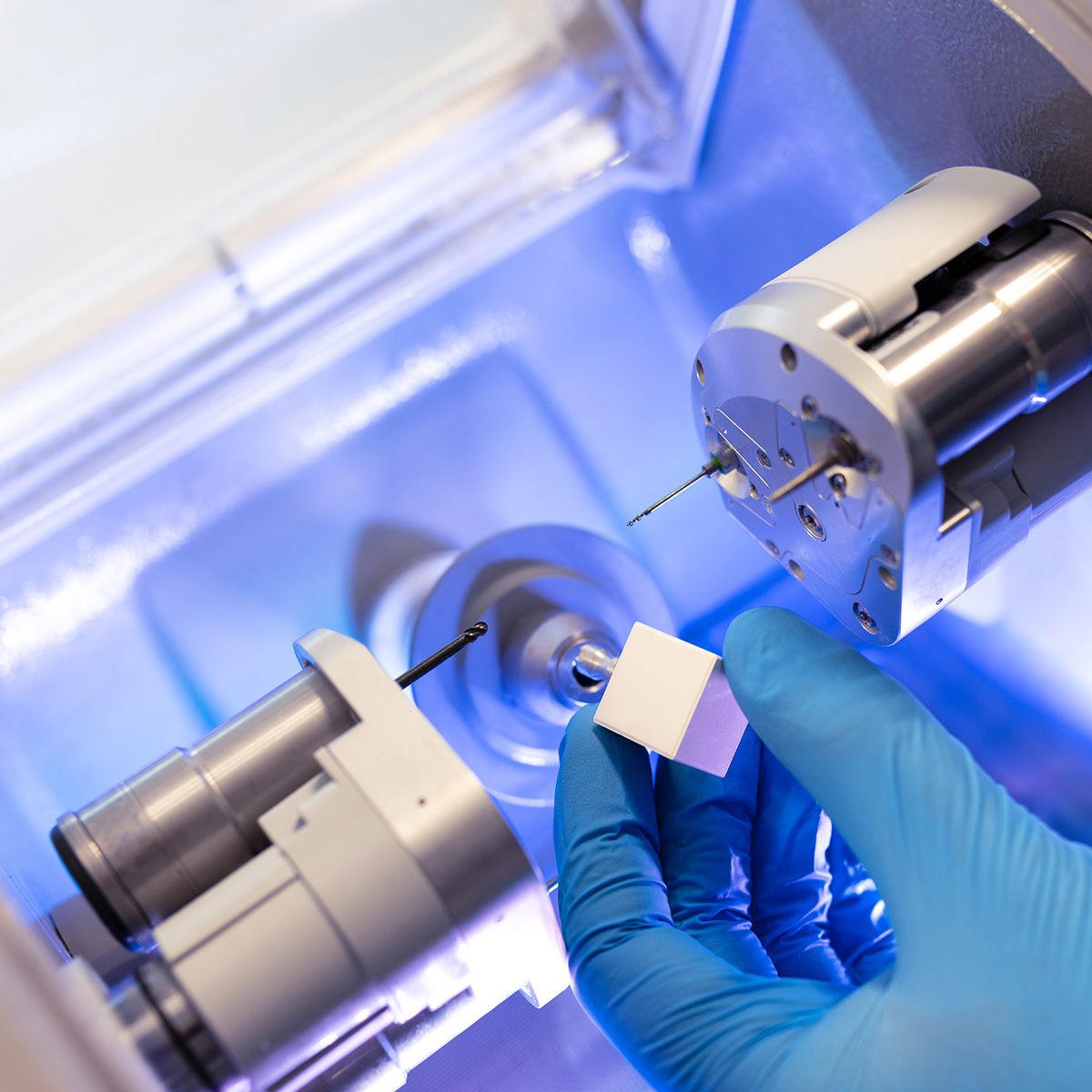
Photolithography
Photomasks & Microfabrication
Photomask blanks, direct-write photomasks, spin coating, lithography, and lift-off processing for semiconductor, MEMS, photonics, and microfluidic applications.
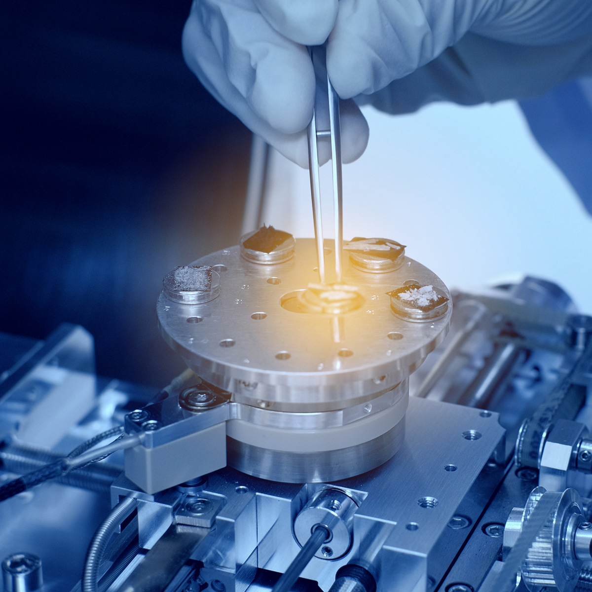
Integrated Manufacturing
One Partner from Starting Substrate to Finished Component
Most optical components pass through several suppliers before they are complete. HEF Photonics brings glass sourcing and fabrication, thin-film optical and conductive coatings, and photolithographic patterning together within a single manufacturing operation.
Fewer handoffs mean less handling of sensitive substrates, shorter lead times, and single-point accountability for the finished part, whether you need one process or the complete sequence.
How We Work Together
Every program starts with the application. Our team reviews the optical, mechanical, environmental, and production requirements, then recommends the substrate, coating design, and patterning approach that fit the component and the budget.
From there, each step can be completed in-house, from material selection through inspection and cleanroom packaging.
- MATERIAL SELECTION
- FABRICATION
- THIN-FILM COATING
- PATTERNING
- INSPECTION
- FINISHED COMPONENT
Use any capability on its own or combine them into a single, integrated workflow.
Why HEF Photonics?
Decades of Thin-Film Experience
More than 50 years of photomask and thin-film manufacturing experience through Telic, combined with Abrisa’s glass fabrication and optical coating expertise.
Broad Spectral Coverage
Coating capabilities from approximately 200 nm in the UV to 20 microns in the far infrared, on a wide range of glass, crystalline, and specialty substrates.
Small to Large-Format Processing
Capabilities range from conventional photomask sizes and thin glass down to approximately 0.03 mm, up to large-format substrates of 50″ × 50″.
Prototype Through Production
Support for rapid development programs as well as repeatable, documented production, with stocking options for frequently used materials.
