
Photolithography & Microfabrication
HEF Photonics provides photomask blanks, precision photomasks, photoresist coating, lithography, lift-off, and related microfabrication services for applications in semiconductor, photonics, MEMS, microfluidics, biomedical devices, and advanced research.
With more than 50 years of experience in photomask and thin-film manufacturing through Telic, HEF Photonics combines substrate preparation, PVD thin-film deposition, spin coating, lithography, patterning, inspection, and cleanroom packaging within a single manufacturing operation. These capabilities can be used individually or combined to support programs from prototype development through production.

Common applications include:
- Photomasks and reticles
- Semiconductor and microelectronics
- MEMS
- Photonics
- Microfluidics and lab-on-a-chip devices
- Biomedical devices and biosensors
- Holographic and diffractive optics
- Flat panel displays
- PCB tooling masters
- Optical alignment and targeting
- Research and development
List lead-in:
- Item
Photomask Blanks
Precision Substrates for Optical & E-Beam Lithography
HEF Photonics manufactures photomask blanks for conventional optical lithography, e-beam lithography, semiconductor development, MEMS, photonics, flat panel displays, microfluidics, and other microfabrication applications.
Photomask-quality substrates are double-side polished and combined with vacuum-deposited, DC-sputtered chrome films in a controlled cleanroom environment. Standard and custom film thicknesses, optical densities, reflectivity levels, substrate materials, and photoresist options are available to match the lithography process and application.
Standard Photomask Blanks
Standard optical lithography blanks are available in sizes from 2" × 2" through 7" × 7" on soda lime, borosilicate, white crown, and synthetic fused silica substrates. Standard substrate specifications include double-side polishing, inspection for glass defects greater than 2 µm, and flatness of ≤15 µm. Custom thicknesses and film specifications are available.

Large-Format Photomask Blanks
For flat panel displays, large-area microfabrication, holography, PCB tooling, and other large-format applications, photomask blanks can be produced in sizes up to 50" × 50". Large-format capabilities can be combined with thin-film deposition and photoresist coating to provide application-specific substrates ready for subsequent lithographic processing.

E-Beam Photomask Blanks
E-beam photomask blanks are available for high-resolution electron-beam lithography and advanced pattern generation. Available substrate materials include soda lime, borosilicate, white crown, and synthetic fused silica, with chrome film and photoresist options including PMMA and negative e-beam resist systems.
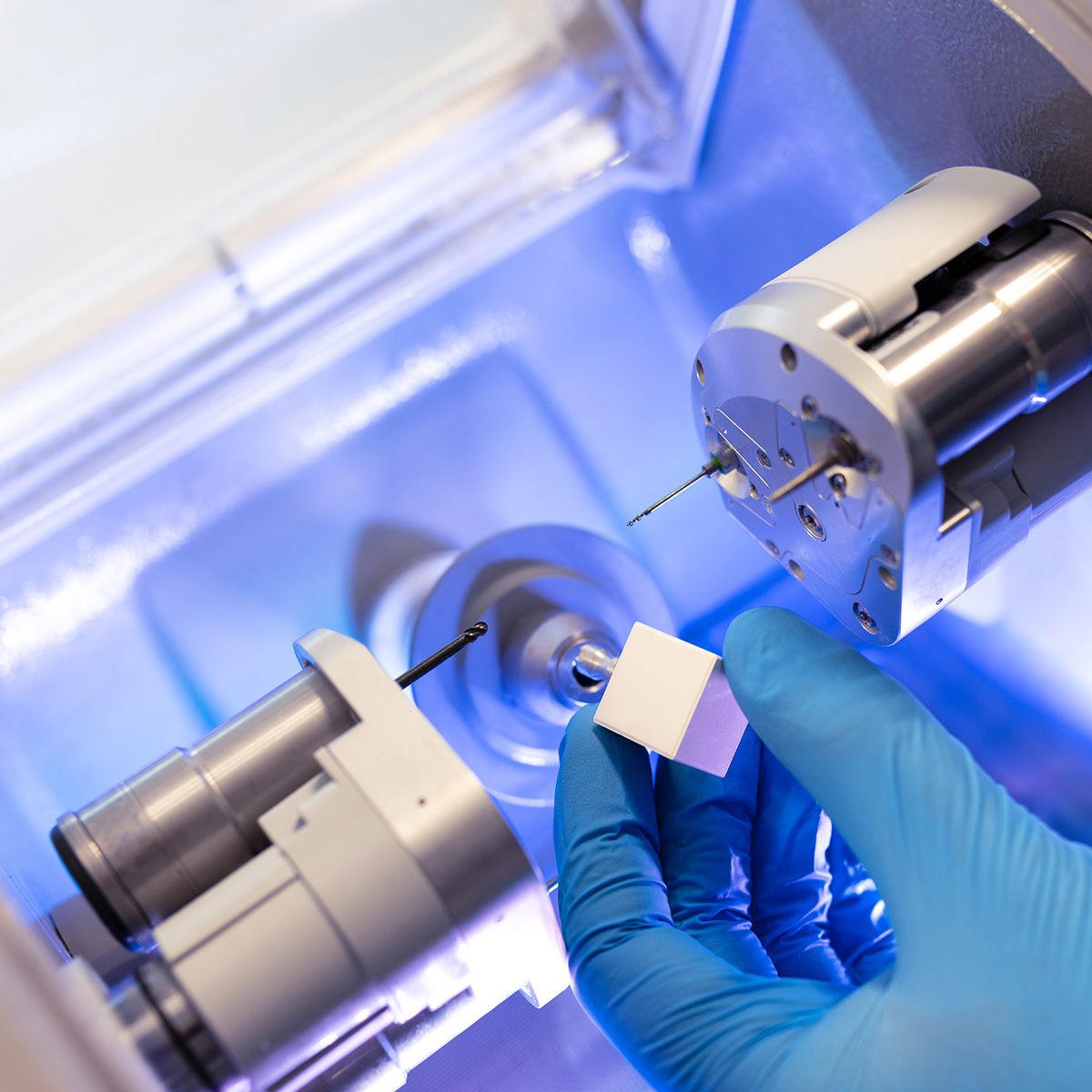
Precision Photomasks
Direct-Write Patterning for Custom Masks & Reticles
In addition to supplying photomask blanks, HEF Photonics manufactures finished patterned photomasks for commercial, defense, biomedical, semiconductor, research, and other microfabrication applications.
Direct-write lithography allows custom patterns to be produced from digital design data without requiring a separate master mask, making the process well suited to prototype development, custom designs, and production photomasks.
Direct-write capabilities include:
- Write areas up to 200 mm × 200 mm
- Minimum feature sizes down to approximately 1 µm
- Mask sizes from 2.5″ × 2.5″ through 7″ × 7″
- Low-reflective chrome
- Iron oxide
- Soda lime and quartz substrates
- Custom photomasks and reticles
- Aperture windows
- Alignment and target patterns
HEF Photonics supports both development and ongoing production requirements, with the appropriate substrate, coating, resolution, and patterning process selected based on the application.
Lithography & Patterning
Precision Pattern Definition for Thin Films & Microfabricated Devices
HEF Photonics provides lithographic patterning services for customers requiring more than a coated or photoresist-covered substrate.
Photolithography can be combined with thin-film deposition, spin coating, mask alignment, etching, and lift-off to create patterned metallic and functional thin-film structures for photonics, sensing, microfluidics, semiconductor development, and other microfabrication applications.
Capabilities include:
- Mask alignment
- Multilayer lithography
- Direct-write pattern generation
- Aperture windows
- Target reticles
- Custom pattern generation
- Patterned thin-film substrates
- Prototype and production processing
By combining these processes within the same manufacturing operation, HEF Photonics can support the component beyond the photomask blank and through the patterned thin-film structure.
Lift-Off Processing
Patterned Metallic & Functional Thin Films
Lift-off processing combines photoresist patterning with thin-film deposition to create defined metallic and functional thin-film features on glass, quartz, silicon, and other compatible substrates.
HEF Photonics combines in-house sputtering, spin coating, lithography, and lift-off processing, reducing the need to move sensitive substrates between multiple suppliers.
Lift-off processing supports custom patterned structures used in:
- Photonic devices
- Sensors
- Microfabricated devices
- Research and development
- Custom metallic thin-film patterns
- Application-specific functional structures
Available materials and achievable feature sizes depend on the substrate, film, geometry, and process requirements.
Spin-Coated Photoresist & BARC
Uniform Coatings from Small Substrates to Large Formats
HEF Photonics provides precision spin coating of positive and negative photoresists, Bottom Anti-Reflective Coatings (BARC), and other specialty polymer materials.
Coating processes support photomasks, holographic mastering, microfluidics, MEMS, micro-optics, semiconductor development, and other applications requiring controlled photoresist thickness and uniformity.
Capabilities include:
- Positive and negative photoresists
- Optical and e-beam resists
- Thick-film photoresist
- BARC
- LOR and related lift-off materials
- Custom coating processes
- Customer-supplied substrates
- Large-format coating up to 50″ × 50″
- Prototype through production quantities
A wide range of commercially available resist systems can be supported based on the customer’s exposure, development, patterning, and final application requirements.
Holographic Blanks
Precision Photoresist-Coated Substrates for Holographic & Diffractive Mastering
HEF Photonics manufactures photomask-quality holographic blanks for grayscale lithography, diffractive optical element (DOE) mastering, high-resolution holography, micro-optical structures, and related applications.
Glass provides a flat, dimensionally stable recording surface, while controlled substrate preparation and photoresist coating help maintain uniformity across the working area.
Holographic blanks combine double-side polished substrates with precision spin-coated photoresist and are available in formats up to 50″ × 50″.
Applications include:
- Security and authentication holograms
- Diffractive Optical Element (DOE) mastering
- Holographic optical components
- Diffraction gratings
- Grayscale lithography
- Micro-optical structures
- Microfluidic master tooling
- Research and development
Large-Area Spin Coating
Large-Format Photoresist-Coated Substrates
Large-format photoresist-coated substrates are available for applications requiring lithographic processing over areas beyond conventional photomask sizes.
HEF Photonics provides large-area spin coating on soda lime, borosilicate, quartz, silicon wafers, and customer-supplied materials for applications including 3D microstructures, microfluidics, MEMS, holography, micro-optics, and advanced research.
Positive, negative, thick-film, BARC, and custom coating processes are available based on the application.
PVD Thin-Film Deposition
Metallic & Dielectric Films for Microfabrication
HEF Photonics provides precision DC and RF magnetron sputtering of metallic and dielectric thin films on glass, quartz, silicon, sapphire, ceramics, and other specialty substrates.
Thin-film deposition can be supplied as a standalone service or integrated with polishing, spin coating, lithography, and lift-off to produce patterned or application-ready components.
For photomask applications, DC-sputtered chrome is available with controlled thickness, optical density, and reflectivity, including low-, mid-, and high-reflective options. Custom chrome thicknesses up to approximately 5 µm are available.
Process Overview
HEF Photonics’ photolithography and microfabrication capabilities can support individual process steps or an integrated manufacturing sequence.
Depending on the application, processing can begin with substrate selection and double-sided polishing to establish the required flatness, parallelism, and surface quality. Metallic or dielectric thin films are then deposited by PVD sputtering as required.
Photoresist or BARC can be applied through controlled spin coating, followed by direct-write or mask-based lithography to define the required pattern. Etching or lift-off processing is then used as applicable to transfer that pattern into the thin film or create the finished patterned structure.
Components are inspected throughout the manufacturing process and can be supplied with custom cleanroom packaging for protection during storage, shipment, and subsequent customer processing.
- SUBSTRATE
- POLISHING
- THIN-FILM DEPOSITION
- SPIN COATING
- LITHOGRAPHY
- ETCH / LIFT-OFF
- INSPECTION
- CLEANROOM PACKAGING
Customers can use any of these processes individually or combine them into an integrated manufacturing workflow.
Advantages of Photolithography
Integrated Microfabrication
HEF Photonics combines substrate preparation, thin-film deposition, spin coating, lithography, lift-off, inspection, and cleanroom packaging within one manufacturing operation. This reduces handling between suppliers and provides greater process continuity from the starting substrate through the finished patterned component.
Standard & Custom Photomask Solutions
Standard photomask blanks are available alongside custom substrate sizes, thicknesses, chrome specifications, reflectivity levels, photoresists, and finished direct-write photomasks. This allows the manufacturing approach to be matched to the customer’s lithography process rather than limiting the application to a standard blank.
Small to Large-Format Processing
Capabilities range from conventional 2-inch photomask blanks to large-format substrates up to 50″ × 50″, supporting applications from semiconductor and MEMS development to flat panel displays, holography, and large-area microfabrication.
Prototype Through Production
Photomask, coating, lithography, and microfabrication processes support rapid development and prototype programs as well as repeatable production requirements.
Custom Engineering Support
Our team works with customers to understand the complete process—including substrate, film, photoresist, exposure method, feature size, pattern geometry, and downstream processing—to develop a manufacturing approach suited to the application.
Photolithography & Microfabrication Services
Photomask Blanks
Standard, large-format, and e-beam photomask blanks with standard and custom chrome and photoresist options.
Precision Photomasks
Direct-write patterned photomasks, reticles, apertures, and custom patterns.
Lithography & Lift-Off
Photolithographic patterning and lift-off processing for custom thin-film structures.
